Experiment
Pulse Code Modulation (PCM)
Objectives:
1- Introduction to PCM and Analog-to-Digital Conversion.
2- To understand the operation theory of pulse coded modulation (PCM).
3- To understand the theory of PCM modulation circuit.
Basic Information:
PCM modulation is a kind of source coding. The meaning of source coding is the conversion from analog signal to digital signal. After converted to digital signal, it is easy for us to process the signal such as encoding, filtering the unwanted signal and so on. Besides, the quality of digital signal is better than analog signal. This is because the digital signal can be easily recovered by using comparator.
Information in an analog form cannot be processed by digital computers so it's necessary to convert them into digital form. PCM is a term which was formed during the development of digital audio transmission standards. Digital data can be transported robustly over long distances unlike the analog data and can be interleaved with other digital data so various combinations of transmission channels can be used.
PCM doesn`t mean any specific kind of compression, it only implies PAM (pulse amplitude modulation) - quantization by amplitude and quantization by time which means digitalization of the analog signal. The range of values which the signal can achieve (quantization) is divided into segments, each segment has a segment representative of the quantization level which lies in the middle of the segment.
The value that a signal has in certain time is called a sample, the process of taking samples is called quantization by time. After quantization by time, it is necessary to conduct quantization by amplitude. Quantization by amplitude means that according to the amplitude of sample one quantization segment is chosen (every quantization segment contains an interval of amplitudes)
PCM modulation is commonly used in audio and telephone transmission. The main
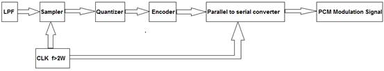
advantage is the PCM modulation only needs 8 kHz sampling frequency to maintain the original quality of audio. Figure 1.1 is the block diagram of PCM modulation. First of all is the low pass filter, which is used to remove the noise in the audio signal. After that the audio signal will be sampled to obtain a series of sampling values. Next, the signal will pass through to quantize the sampling values. Then the signal will pass through an encoder to encode the quantization values and then convert to digital signal. In fact, the process of quantization can be achieved at one time by A/D converter. However, we should pay attention on the quantization levels. For example if the bits for PCM modulation is 3, then the quantization levels is 2^3 =8, which is 8 steps. If the bits for PCM are 4, then the quantization levels is 2^4 =16, which is 16 steps. The increasing of bits of PCM modulation will prevent the signal from distortion, but the bandwidth will also increase due to the increasing of the capacity of data. the encoder utilizes n output terminals, therefore, we need to convert the parallel data to serial data, which is the way that satisfy the data format of PCM modulation.
Figure 1.1 Block diagram of Pulse Code modulation.
Modulation process is executed in three steps:
1. Sampling
2. Quantizing
3. Coding
Sampling:
A band limited signal can be reconstructed exactly if it is sampled at a rate at least twice the maximum frequency (2ωm) component in it.

Figure 1.2 Spectrum of band limited signal g(t)
The maximum frequency component of g(t) is Fm, to recover the signal g(t) exactly from its samples it has to be sampled at a rate Fs ≥ 2Fm. The minimum required sampling rate Fs = 2Fm is called Nyquist rate
Proof:
Let g(t) be a band limited signal whose bandwidth is Fm
(ωm = 2πFm).
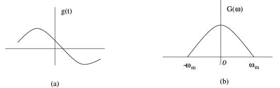
Figure 1.3: (a) Original signal g(t) (b) Spectrum G(ω)
δT (t) is the sampling signal with Fs = 1/T > 2Fm.
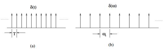
Figure 1.4 : (a) sampling signal T(t) (b) Spectrum(ω)
Let gs(t) be the sampled signal. Its Fourier Transform Gs(ω) is given by

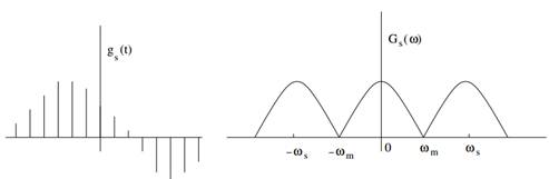
Figure 1.5: (a) sampled signal gs(t) (b) Spectrum Gs(ω)
If ωs = 2ωm, i.e., T = 1/2Fm. Therefore, Gs(ω) is given by:
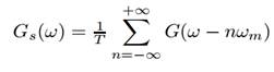
To recover the original signal G(ω):
1- Filter with a Gate function, H2ωm(ω) of width 2ωm
2- Scale it by T
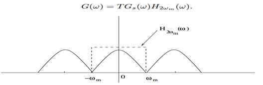
Figure 1.6: Recovery of signal by faltering with a filter of width 2ωm
Aliasing:
Aliasing is a phenomenon where the high frequency components of the sampled signal interfere with each other. because of inadequate sampling ωs < 2ωm.
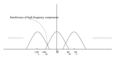
Figure 1.7: Aliasing due to inadequate sampling
Aliasing leads to distortion in recovered signal. This is the reason why sampling frequency should be at least twice the bandwidth of the signal.
Oversampling:
In practice signal are oversampled, where Fs is significantly higher than Nyquist rate to avoid aliasing.
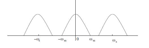
Figure 1.8: Oversampled signal-avoids aliasing
2. Quantization :
a- Uniform

Figure 1.9 Block diagram for sampling, quantization, and encoding
• Sampling: take samples at time nT
T: sampling period;
Fs = 1/T: sampling frequency.
• Quantization: map amplitude values into a set of discrete values kQ; where k is integer
Q: quantization interval
• Binary Encoding – Convert each quantized value into a binary codeword
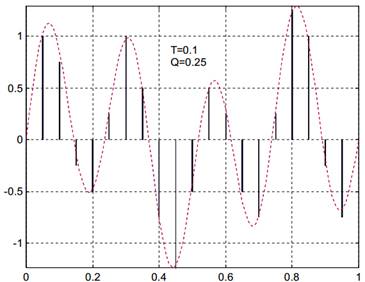
Figure 1.10 Analog to digital convert.
How to Determine sampling period and quantization interval?
• T (or Fs) depends on the signal frequency range.
– A fast varying signal should be sampled more frequently!
– Theoretically governed by the Nyquist sampling theorem
• Fs > 2Fm (Fm is the maximum signal frequency)
• Q depends on the dynamic range of the signal amplitude and perceptual sensitivity Q and the signal range D determine bits/sample R
• 2R =D/Q
• One can trade off T (or Fs) and Q (or R), lower R è higher Fs ; higher R è lower Fs.
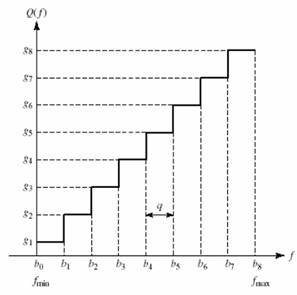
Figure 1.11 Uniform quantization.
• Applicable when the signal is in a finite range (Fmin,Fmax )
• The entire data range is divided into L equal intervals of length Q (known as quantization interval or quantization level)
![]()
• interval I is mapped to the middle value of this interval .
• We store/send only the index of quantized value.
•Index of quantized value
![]()
•Quantized value
![]()
As stated before, in PCM, the information signal x(t) is first sampled with the appropriate sampling frequency (sampling frequency Fs ≥ 2×highest frequency of the information signal (Fx) ), then the sampled levels are quantized to appropriate quantization levels. In the last step, each quanta level is demonstrated by a two-code word, that is by a finite number of {0,1} sequence. After this step, the signal is called as PCM wave.
If the max and min amplitude values of information signal x(t) are Amax and Amin, respectively, and if n-digit code words will be used, then the quantizing interval/pace “a” becomes:
![]()
Figure 1.12: Sampling and Quantizing of an analog signal and indication of
corresponding PCM waveforms.
In Figure 2, the signal is divided into 16 amplitude levels (0-1.5) between its max and min values. Therefore, n=4 and the quantizing pace a =0.1. If the quantizing levels are selected equally, then this is called as “linear quantizing”. Figure 3 shows an example to the linear quantizing.

Figure 1.13. Linear/Uniform Quantizing
A little information about the PCM Encoder module on the Emona FOTEx:
The PCM encoder module uses a PCM encoding and decoding chip (called a codec) to convert analog voltages between -2.5V and +2.5V to a 7-bit binary number. with seven bits, its possible to produce 128 different number between 0000000 and 1111111 inclusive, this in turn means that there are 128 quantization levels ( one for each number).
Each binary number is available on the PCM encoder modules output in serial from in 8-bit frames. The binary number's most significant bit is sent first and so is found on bit-7 of the frame. The numbers next most significant bit is sent next and so on to the least significant bit (which is found on bit-1 of the frame). Bit-0 of the frame is a frame synchronization but used by the PCM decoder module to find the beginning of each frame. It simply alternates between 0-1 on successive frames.
The PCM encoder module also outputs a separate Frame Synchronization singal FS that goes high at the same time as the frame's synchronization but is outputted. The FS output is not needed by the PCM decoder module and has been provided on the FOTEx purely for the Scope triggering.
Figure 2.1 below shows and example of three frames of a PCM encoder module's output data together with its clock input and its FS output buts7to 1 are shown as both a 0 and a 1 because they could be either depending on the size of analog input.

Figure 1.14
For this experiment you will use the PCM encoder module on the EMONA FOTEx to convert the following to PCM a fixed DC voltage a variable dc voltage and a continuously changing signal in the process you will verify the operation of PCM encoding.
Experiment Equipment:
1- Emona FOTEx.
2- NI-elivs II.
3- LabVIEW(oscilloscope, FunctionGenerator ).
4- You must download runtime engine.
Procedure:
An introduction to PCM encoding using a static DC voltage.
This set-up can be represented by the block digram in figure 2.2 below the pcm encoder module is clocked by the master signal modules 10khz digital output and its analog input is connected to 0V DC
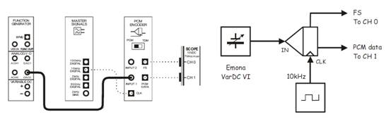
Figure 1.15 Block diagram PCM on EMONA FOTEx.
|
Frequency |
Vin |
Vout |
|
10Khz |
5 |
|
|
10Khz |
10 |
|
|
10Khz |
15 |
|
|
10Khz |
20 |
|
|
10Khz |
25 |
|

|
Frequency |
Vin |
Vout |
|
10Khz |
5 |
|
|
15Khz |
5 |
|
|
20Khz |
5 |
|
|
25Khz |
5 |
|
|
30Khz |
5 |
|
|
Frequency |
Vin |
Vout |
|
10Khz |
5 |
|
|
15Khz |
10 |
|
|
20Khz |
15 |
|
|
25Khz |
20 |
|
|
30Khz |
25 |
|